Semiconductor Engineering
How the chips inside almost every modern electronic device get designed and manufactured.
FIG. 01 — SEMICONDUCTOR ENGINEERING
What It Is
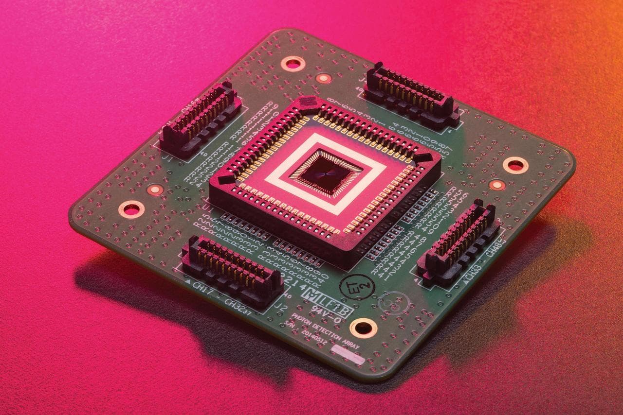
Semiconductor engineering is about designing and manufacturing the chips that power almost every modern electronic device — working at the scale of individual circuits and materials, not a finished product. It combines electrical engineering, materials science, and precision manufacturing.
What Engineers Work On
Semiconductor engineers work at a scale where the material itself is the design. Some work on the circuit — laying out transistors, checking timing, and simulating a block long before any silicon exists. Others work on the process, tuning the sequence of deposition, patterning, and etching steps that build a chip layer by layer, and hunting the reasons a wafer came out wrong. Both sides live on data: enormous amounts of measurement, and the statistics needed to tell a real effect from noise.
Real-World Examples
- Microchip and processor design
- Semiconductor fabrication process engineering
- Chip testing and quality verification
- Materials engineering for semiconductor manufacturing
Common Misconceptions
Tap a card to see the reality behind each one.
Myth: Semiconductor engineers build computers.
Reality: They build what's inside the chip. A finished computer is many layers of abstraction above where this work happens.
Myth: It's one job.
Reality: Design and process are close to separate professions. One simulates circuits at a desk; the other runs and debugs a fabrication line.
Myth: Modern fabs are fully automated, so there's little to do.
Reality: Automation runs the steps. Engineers decide what the steps should be and work out why yield dropped when nothing obvious changed.
Myth: You need a PhD to get in.
Reality: Research roles often expect one, but a great deal of design, test, and process work is done by people with a bachelor's or master's.
A Day in the Life
For design roles, most of the day is simulation and analysis at a computer, punctuated by design reviews. For process and yield roles, it's a mix of data analysis and time in or beside the fab, following experiments through and reacting when a tool drifts. Both sides are shaped by long cycle times — a wafer takes weeks to work through a line, so today's experiment answers a question you asked some time ago.
One illustrative example day, not a guaranteed schedule — real days vary a lot by employer, role, and industry.
Line review
Checking overnight measurements on the wafers moving through the steps you own. (This example follows a process engineer — a chip design role spends almost the whole day at a computer.)
Checking overnight measurements on the wafers moving through the steps you own. (This example follows a process engineer — a chip design role spends almost the whole day at a computer.)
Gowning up to look at a tool that's drifting out of its normal range, alongside the equipment technicians.
Writing a script to compare yield across tools and batches, to tell a real effect from noise.
Designing a small experiment on a deposition step, knowing the results won't be back for weeks.
Meeting with design and test engineers about a failure pattern showing up in finished chips.
Documenting today's changes for the next shift, since the line doesn't stop overnight.
Would you be patient with work where an experiment you start today might not tell you anything for weeks?
Typical Projects
- Designing and simulating a circuit block against timing, power, and area targets
- Tuning a deposition or etch step to hit a target thickness or profile
- Investigating why yield dropped on a particular product or tool
- Developing test procedures that catch defective chips before they ship
- Characterising a new material or process and documenting how it behaves
Getting Ready
Useful Subjects
- Physics
- Calculus
- Chemistry
- Computer science or programming, if offered
- Statistics, if offered
Helpful Skills
- Comfort with physics and chemistry at a level below the visible, since behaviour comes from material and quantum effects
- Strong statistics, because yield and process control are statistical problems before they are physical ones
- Programming and scripting, since analysing process and test data by hand isn't practical
- Patience with long feedback loops, as a change to a process can take weeks to show up in results
- Methodical debugging, because a defect can come from any of hundreds of steps
Where This Field Shows Up
Industries
- Chip designers and fabless semiconductor companies
- Semiconductor foundries and integrated manufacturers
- Semiconductor equipment and materials suppliers
- Research laboratories and university facilities
- Companies designing custom silicon for their own products
Related Majors
- Electrical Engineering (with a semiconductor focus)
- Materials Science and Engineering (some overlap)
- Computer Engineering (some overlap)
Career Explorer
Process Engineer
Owns one or more fabrication steps and keeps them on target, run after run.
Yield Engineer
Finds out why some chips fail, and which step or tool is responsible.
Chip Design or Verification Engineer
Designs circuit blocks, or proves through simulation that a design works before it's manufactured.
Test Engineer
Develops the tests that catch defective chips before they ship.
Weighing It Up
Advantages
- The work sits underneath nearly all modern technology, so its reach is unusually wide
- It's genuinely deep technical work, with room to specialise a long way
- Design and process paths are different enough that one may suit you when the other doesn't
- Skills in statistics and process control transfer to other high-precision manufacturing
Challenges
- Feedback loops are long, which makes iteration slow compared with software or mechanical work
- The industry is capital-intensive and cyclical, and hiring moves with that cycle
- Fabs are concentrated in particular regions, so location options can be limited
- The learning curve is steep, and much of the practical knowledge is specific to one company's process
Things People Dislike
- Waiting weeks for a wafer to tell you whether an idea worked
- Cleanroom protocol, gowning, and the restrictions that come with it
- Chasing yield problems with hundreds of plausible causes and thin evidence
- On-call and shift coverage when a production line can't be allowed to stop
How Competitive Is It?
The U.S. Bureau of Labor Statistics doesn't publish a separate job-outlook projection for semiconductor engineering — the people doing this work are counted under electrical, computer hardware, materials, and other engineering occupations, so there's no government growth figure specific to this field. Hiring in the industry moves with its investment cycle, which can swing up and down, and fabrication plants are concentrated in particular regions of a few countries, so where you live matters more here than in most fields — research the current situation in the places you'd consider working.
What You Could Earn
No separate U.S. Bureau of Labor Statistics category exists for semiconductor engineering — it's usually pursued through electrical, computer, or materials engineering. See the Electrical Engineering page for related, sourced salary data.
Try It Yourself
- Look up a photo of a chip under a microscope (called a die shot) and try to spot repeated blocks, like memory
- Build a simple circuit on a breadboard with an LED and a transistor, and see how the transistor acts as a switch
- Try the logic gates simulation on this site and work out how gates combine into something that can add
Questions to Ask Yourself
- Am I patient enough for experiments that take weeks to give an answer?
- Would I enjoy working at a scale I can only see through measurements and data?
- Would I be okay following strict cleanroom procedures, or would I rather work in a design role at a computer?
- Would I be willing to live where chip companies and fabs are located?
What Can I Do Next?
Grade level: High school
Grade systems vary by country — pick whichever tab is the closest match for where you are.
Not saved anywhere. (just for this visit — nothing is stored beyond your browser tab).
A project to try
Build logic gates from transistors on a breadboard, then combine them into a small circuit like a half adder.
A tool to learn
A breadboard, a few transistors and LEDs, and a free browser-based circuit simulator like Falstad's.
A club or activity
Take physics or an electronics class, or do a science fair project on electronics, if your school offers them.
How to actually find one near you →